
Allocate space before selecting layers
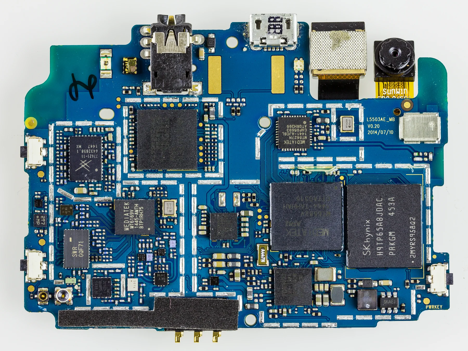
Draw the enclosure, battery, camera volumes, antenna regions, shield boundaries and connector insertion envelopes on one mechanical view. The usable routing area is what remains after these constraints, not the outline area quoted on a drawing. A small shift in a connector can change several escape paths at once.
Create a component escape sketch for the most congested packages. Count the usable routing corridors and identify which signals need an immediate layer transition. This makes the decision between one buildup layer and a deeper structure measurable.
Treat the radio region as a controlled layout
Nordic's nRF52832 reference guidance explains that changes around RF matching circuitry can change its behavior. The practical implication for a mixed smartphone board is to protect validated RF geometry while redistributing digital escape routes around it.
A thinner buildup dielectric or additional ground copper can alter the electromagnetic environment. Record radio keepouts and reference planes in the stackup review, and recheck them when a fabrication proposal changes layer thickness or material.
Resolve the board versus assembly tradeoff
Placing more components under shields may save outline area while restricting probing, inspection and rework. Agree on which measurements must remain accessible after assembly. Include shield attachment, thermal interfaces and component height in the same placement review as microvia routing.
- Mark processor escape nets that drive the HDI requirement.
- Reserve camera and display connector routing before filling nearby space.
- Review battery charging heat with the enclosure team.
- Identify test access that survives shields and final assembly.
Use an evidence based release gate
For the first build, retain the approved stackup, via span drawing and the exact RF layout revision. Compare connectivity, interface operation and thermal behavior against the intended use modes: charging, camera capture, wireless transmission and sustained computation. A board that boots is only the beginning of this review.
If the next revision moves a shield, antenna contact or power converter, treat the change as an electrical and mechanical review item even when the schematic is unchanged.
Adjacent-layer access, one connection at a time
Dielectric · geometry + material
Core or build-up dielectric
Illustrative only. Copper thickness, dielectric construction and via spans require a reviewed stackup.
Common questions
Does every smartphone board require any-layer HDI?
No. The package escape, available area and interface routing determine the need. Demonstrate the bottleneck before adopting a more complex via structure.
Can a reference RF layout be shrunk with the rest of the board?
Do not assume so. Preserve the device supplier's critical geometry and use RF simulation or measurement to evaluate changes in its surroundings.
References & further reading
Method & assumptions · General design guidance. Validate the proposed construction and acceptance criteria for your project.